 | –≠–ª–µ–∫—Ç—Ä–æ–Ω–Ω—ã–π –∫–æ–º–ø–æ–Ω–µ–Ω—Ç: 24C04A-P | –°–∫–∞—á–∞—Ç—å:  PDF PDF  ZIP ZIP |

©
1998 Microchip Technology Inc.
DS11183E-page 1
24C04A
FEATURES
∑ Low power CMOS technology
∑ Hardware write protect
∑ Two wire serial interface bus, I
2
CTM compatible
∑ 5.0V only operation
∑ Self-timed write cycle (including auto-erase)
∑ Page-write buffer
∑ 1 ms write cycle time for single byte
∑ 1,000,000 Erase/Write cycles guaranteed
∑ Data retention >200 years
∑ 8-pin DIP/SOIC packages
∑ Available for extended temperature ranges
DESCRIPTION
The Microchip Technology Inc. 24C04A is a 4K bit
Electrically Erasable PROM. The device is organized
as with a standard two wire serial interface. Advanced
CMOS technology allows a significant reduction in
power over NMOS serial devices. A special feature
provides hardware write protection for the upper half of
the block. The 24C04A has a page write capability of
up to eight bytes, and up to four 24C04A devices may
be connected to the same two wire bus.
This device offers fast (1ms) byte write and
extended (-40
∞
C to 125
∞
C) temperature operation.
It is recommended that all other applications use
Microchip's 24LC04B.
- Commercial (C):
0∞C to
+70∞C
- Industrial (I):
-40∞C to
+85∞C
- Automotive (E):
-40∞C to +125∞C
PACKAGE TYPES
BLOCK DIAGRAM
24C04A
24C04A
A0
A1
A2
V
SS
1
2
3
4
8
7
6
5
V
CC
WP
SCL
SDA
A0
A1
A2
V
SS
1
2
3
4
8
7
6
5
V
CC
WP
SCL
SDA
DIP
8-lead
SOIC
14-lead
SOIC
24C04A
SDA
NC
Vcc
WP
NC
SCL
NC
Vss
NC
A0
A1
NC
A2
NC
1
2
3
4
5
6
7
14
13
12
11
10
9
8
Vcc
Vss
SDA
SCL
Data
Buffer
(FIFO)
Data Reg.
V
PP
R/W Amp
Memory
Array
A
d
d
r
e
s
s
P
o
i
n
t
e
r
A0 to
A7
Increment
A8
Slave Addr.
Control
Logic
A0 A1 A2 WP
4K 5.0V I
2
C
TM
Serial EEPROM
I
2
C is a trademark of Philips Corporation.

24C04A
DS11183E-page 2
©
1998 Microchip Technology Inc.
1.0
ELECTRICAL CHARACTERISTICS
1.1
Maximum Ratings*
V
CC
...................................................................................7.0V
All inputs and outputs w.r.t. V
SS
............... -0.6V to V
CC
+1.0V
Storage temperature ..................................... -65∞C to +150∞C
Ambient temp. with power applied................. -65∞C to +125∞C
Soldering temperature of leads (10 seconds) ............. +300∞C
ESD protection on all pins................................................4 kV
*Notice:
Stresses above those listed under "Maximum ratings"
may cause permanent damage to the device. This is a stress rat-
ing only and functional operation of the device at those or any
other conditions above those indicated in the operational listings
of this specification is not implied. Exposure to maximum rating
conditions for extended periods may affect device reliability.
TABLE 1-1:
PIN FUNCTION TABLE
Name
Function
A0
No Function - Must be connected to
V
CC
or V
SS
A1, A2
Chip Address Inputs
V
SS
Ground
SDA
Serial Address/Data I/O
SCL
Serial Clock
WP
Write Protect Input
V
CC
+5V Power Supply
TABLE 1-2:
DC CHARACTERISTICS
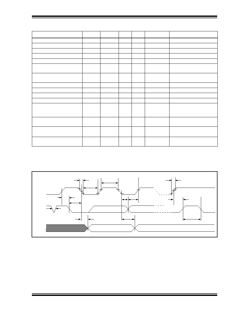
FIGURE 1-1:
BUS TIMING START/STOP
V
CC
= +5V (
±
10%)
Commercial (C): Tamb = 0
∞
C to +70
∞
C
Industrial (I):
Tamb = -40
∞
C to +85
∞
C
Automotive (E):
Tamb = -40
∞
C to +125
∞
C
Parameter
Symbol
Min.
Max.
Units
Conditions
V
CC
detector threshold
V
TH
2.8
4.5
V
SCL and SDA pins:
High level input voltage
Low level input voltage
Low level output voltage
V
IH
V
IL
V
OL
V
CC
x 0.7
-0.3
V
CC
+ 1
V
CC
x 0.3
0.4
V
V
V
I
OL
= 3.2 mA (SDA only)
A1 & A2 pins:
High level input voltage
Low level input voltage
V
IH
V
IL
V
CC
- 0.5
-0.3
V
CC
+ 0.5
0.5
V
V
Input leakage current
I
LI
--
10
µ
A
V
IN
= 0V to V
CC
Output leakage current
I
LO
--
10
µ
A
V
OUT
= 0V to V
CC
Pin capacitance
(all inputs/outputs)
C
IN
,
C
OUT
--
7.0
pF
V
IN
/V
OUT
= 0V (Note)
Tamb = +25∞C, f = 1 MHz
Operating current
I
CC
Write
--
3.5
mA
F
CLK
= 100 kHz, program cycle time = 1 ms,
Vcc = 5V, Tamb = 0∞C to +70∞C
I
CC
Write
--
4.25
mA
F
CLK
= 100 kHz, program cycle time = 1 ms,
Vcc = 5V, Tamb = (I) and (E)
I
CC
Read
--
750
µ
A
V
CC
= 5V, Tamb= (C), (I) and (E)
Standby current
I
CCS
--
100
µ
A
SDA=SCL=V
CC
=5V (no PROGRAM active)
WP/TEST = V
SS
, A0, A1, A2 = V
SS
Note: This parameter is periodically sampled and not 100% tested
T
SU
:
STA
T
HD
:
STA
V
HYS
T
SU
:
STO
START
STOP
SCL
SDA
©
1998 Microchip Technology Inc.
DS11183E-page 3
24C04A
TABLE 1-3:
AC CHARACTERISTICS
FIGURE 1-2:
BUS TIMING DATA
Parameter
Symbol
Min.
Typ
Max.
Units
Remarks
Clock frequency
F
CLK
--
--
100
kHz
Clock high time
T
HIGH
4000
--
--
ns
Clock low time
T
LOW
4700
--
--
ns
SDA and SCL rise time
T
R
--
--
1000
ns
SDA and SCL fall time
T
F
--
--
300
ns
START condition hold time
T
HD
:S
TA
4000
--
--
ns
After this period the first
clock pulse is generated
START condition setup time
T
SU
:S
TA
4700
--
--
ns
Only relevant for repeated
START condition
Data input hold time
T
HD
:D
AT
0
--
--
ns
Data input setup time
T
SU
:D
AT
250
--
--
ns
Data output delay time
T
AA
300
--
3500
(Note 1)
STOP condition setup time
T
SU
:S
TO
4700
--
--
ns
Bus free time
T
BUF
4700
--
--
ns
Time the bus must be free
before a new transmission
can start
Input filter time constant
(SDA and SCL pins)
T
I
--
--
100
ns
Program cycle time
T
WC
--
.4
1
ms
Byte mode
.4N
N
ms
Page mode, N=# of bytes
Endurance
--
1M
--
--
cycles
25
∞
C, Vcc = 5.0V, Block
Mode (Note 2)
Note 1: As transmitter the device must provide this internal minimum delay time to bridge the undefined region (min-
imum 300 ns) of the falling edge of SCL to avoid unintended generation of START or STOP conditions.
2: This parameter is not tested but guaranteed by characterization. For endurance estimates in a specific appli-
cation, please consult the Total Endurance Model which can be obtained on our website.
T
SU
:
STA
T
F
T
LOW
T
HIGH
T
R
T
HD
:
DAT
T
SU
:
DAT
T
SU
:
STO
T
HD
:
STA
T
BUF
T
AA
T
AA
T
SP
T
HD
:
STA
SCL
SDA
IN
SDA
OUT

24C04A
DS11183E-page 4
©
1998 Microchip Technology Inc.
2.0
FUNCTIONAL DESCRIPTION
The 24C04A supports a bidirectional two wire bus and
data transmission protocol. A device that sends data
onto the bus is defined as transmitter, and a device
receiving data as receiver. The bus has to be con-
trolled by a master device which generates the serial
clock (SCL), controls the bus access, and generates
the START and STOP conditions, while the 24C04A
works as slave. Both master and slave can operate as
transmitter or receiver but the master device deter-
mines which mode is activated.
Up to four 24C04As can be connected to the bus,
selected by A1 and A2 chip address inputs. A0 must
be tied to V
CC
or V
SS
.
3.0
BUS CHARACTERISTICS
The following bus protocol has been defined:
∑ Data transfer may be initiated only when the bus
is not busy.
∑ During data transfer, the data line must remain
stable whenever the clock line is HIGH. Changes
in the data line while the clock line is HIGH will be
interpreted as a START or STOP condition.
Accordingly, the following bus conditions have been
defined (Figure 3-1).
3.1
Bus not Busy (A)
Both data and clock lines remain HIGH.
3.2
Start Data Transfer (B)
A HIGH to LOW transition of the SDA line while the
clock (SCL) is HIGH determines a START condition.
All commands must be preceded by a START condi-
tion.
3.3
Stop Data Transfer (C)
A LOW to HIGH transition of the SDA line while the
clock (SCL) is HIGH determines a STOP condition. All
operations must be ended with a STOP condition.
3.4
Data Valid (D)
The state of the data line represents valid data when,
after a START condition, the data line is stable for the
duration of the HIGH period of the clock signal.
The data on the line must be changed during the LOW
period of the clock signal. There is one clock pulse per
bit of data.
Each data transfer is initiated with a START condition
and terminated with a STOP condition. The number of
the data bytes transferred between the START and
STOP conditions is determined by the master device
and is theoretically unlimited.
3.5
Acknowledge
Each receiving device, when addressed, is obliged to
generate an acknowledge after the reception of each
byte. The master device must generate an extra clock
pulse which is associated with this acknowledge bit.
The device that acknowledges has to pull down the
SDA line during the acknowledge clock pulse in such a
way that the SDA line is stable LOW during the HIGH
period of the acknowledge related clock pulse. Of
course, setup and hold times must be taken into
account. A master must signal an end of data to the
slave by not generating an acknowledge bit on the last
byte that has been clocked out of the slave. In this
case, the slave must leave the data line HIGH to enable
the master to generate the STOP condition.
Note:
The 24C04A does not generate any
acknowledge bits if an internal program-
ming cycle is in progress.
FIGURE 3-1:
DATA TRANSFER SEQUENCE ON THE SERIAL BUS
SCL
SDA
(A)
(B)
(D)
(D)
(A)
(C)
START
CONDITION
ADDRESS OR
ACKNOWLEDGE
VALID
DATA
ALLOWED
TO CHANGE
STOP
CONDITION

©
1998 Microchip Technology Inc.
DS11183E-page 5
24C04A
4.0
SLAVE ADDRESS
The chip address inputs A1 and A2 must be externally
connected to either V
CC
or ground (V
SS
), thereby
assigning a unique address to each device. A0 is not
used on the 24C04A and must be connected to either
V
CC
or V
SS
. Up to four 24C04A devices may be con-
nected to the bus. Chip selection is then accomplished
through software by setting the bits A1 and A2 of the
slave address to the corresponding hard-wired logic lev-
els of the selected 24C04A. After generating a START
condition, the bus master transmits the slave address
consisting of a 4-bit device code (1010), followed by the
chip address bits A0, A1 and A2. The seventh bit of that
byte (A0) is used to select the upper block (addresses
100--1FF) or the lower block (addresses 000--0FF) of
the array.
The eighth bit of the slave address determines if the
master device wants to read or write to the 24C04A
(Figure 4-1).
The 24C04A monitors the bus for its corresponding
slave address all the time. It generates an acknowl-
edge bit if the slave address was true and it is not in a
programming mode.
FIGURE 4-1:
SLAVE ADDRESS
ALLOCATION
SLAVE ADDRESS
1
0
1
0
A2
A1
A0
R/W
A
START
READ/WRITE
5.0
BYTE PROGRAM MODE
In this mode, the master sends addresses and one
data byte to the 24C04A.
Following the START signal from the master, the device
code (4-bits), the slave address (3-bits), and the R/W
bit, which is logic LOW, are placed onto the bus by the
master. This indicates to the addressed 24C04A that a
byte with a word address will follow after it has gener-
ated an acknowledge bit. Therefore the next byte trans-
mitted by the master is the word address and will be
written into the address pointer of the 24C04A. After
receiving the acknowledge, the master device trans-
mits the data word to be written into the addressed
memory location. The 24C04A acknowledges again
and the master generates a STOP condition. This ini-
tiates the internal programming cycle (Figure 6-1).